CVD Graphene on SiO2 Substrate
₹ 23805 – ₹ 145475Price range: ₹ 23805 through ₹ 145475 exc. gst
CVD Graphene on SiO2 Substrate
YAAVIK MATERIALS AND ACS MATERIALS PRESENTS CVD Graphene on SiO2 Substrate in India.
Product Detail
CAS No.: 7782-42-5 (graphene), 7631-86-9 (silicon dioxide), 7440-21-3 (silicon)
| Sheet Resistance |
<600Ω/sq |
| Custom Order |
<300Ω/sq |
| Transparency |
>95% |
We are thrilled to be a part of the exciting research and innovation involving graphene. We are committed to providing a full range of outstanding graphene products, including these high-quality CVD Graphene sheets on SiO2 substrate. Our proven, proprietary method for CVD transfer of graphene onto P-type, 1-10 Ω·CM silicon dioxide substrate includes the following steps:
- Growing monolayer graphene on copper foil
- Depositing onto SiO2 via PMMA
- Curing
- Removing Cu by etching process
- Washing PMMA/graphene in DI water
- Redepositing PMMA/graphene onto silicon dioxide substrate followed by curing
- Removing PMMA with acetone
The result is a superior product in every way.
- Our process allows us to create graphene sheets in various sizes, from 0.5 cm x 0.5 cm to 1” x 1”.
- Monolayer sheets or multilayer sheets are available: 1, 2, 3-5, or 6-8 layers.
- The thickness and quality of the films is precisely controlled using Raman spectroscopy.
- Graphene films are continuous with minimal holes and cracks.
CVD Graphene on SiO2 substrate is just one of many graphene products and services offered . Others include:
- Large size graphene on copper foil in sheets up to 30 cm x 20 cm
- Double or multilayer graphene sheets on various substrates
- Pretreated graphene coated in PMMA; with simple steps‚ you can easily transfer graphene to other substrates
- Graphical graphene customized according to graphics mask supplied by customers
- Customized services providing different floors‚ different sizes of graphene, various graphene transfer services, nitrogen-doped graphene, etc;
Graphene on silicon dioxide (300nm)/Si substrate (p-type, 1-10 Ω·cm) was prepared by the following steps:
- Monolayer graphene grown on copper foil
- Deposit PMMA and cure
- Remove Cu by etching process
- Wash PMMA/Graphene in DI water
- Redeposit PMMA/Graphene onto silicon dioxide substrate and cure
- Remove PMMA with acetone

Wafer Structure
| CVD Graphene |
Substrate** |
| 1cm x 1cm |
1.5cm x 1.5cm, thickness: 300+/-20nm SiO2 / 670+/-20um Si |
| 1inch x 1inch |
3.0cm x 3.0cm, thickness: 300+/-20nm SiO2 / 670+/-20um Si |
| 3cm x 3cm |
3.5cm x 3.5cm, thickness: 300+/-20nm SiO2 / 670+/-20um Si |
| 7cm x 7cm |
Diameter: 4inch, thickness: 300+/-20nm SiO2 / 500+/-20um Si |
| DIA: 4inch |
Diameter: 4inch, thickness: 300+/-20nm SiO2 / 500+/-20um Si |
**Substrate is available for purchase too. Order now>>
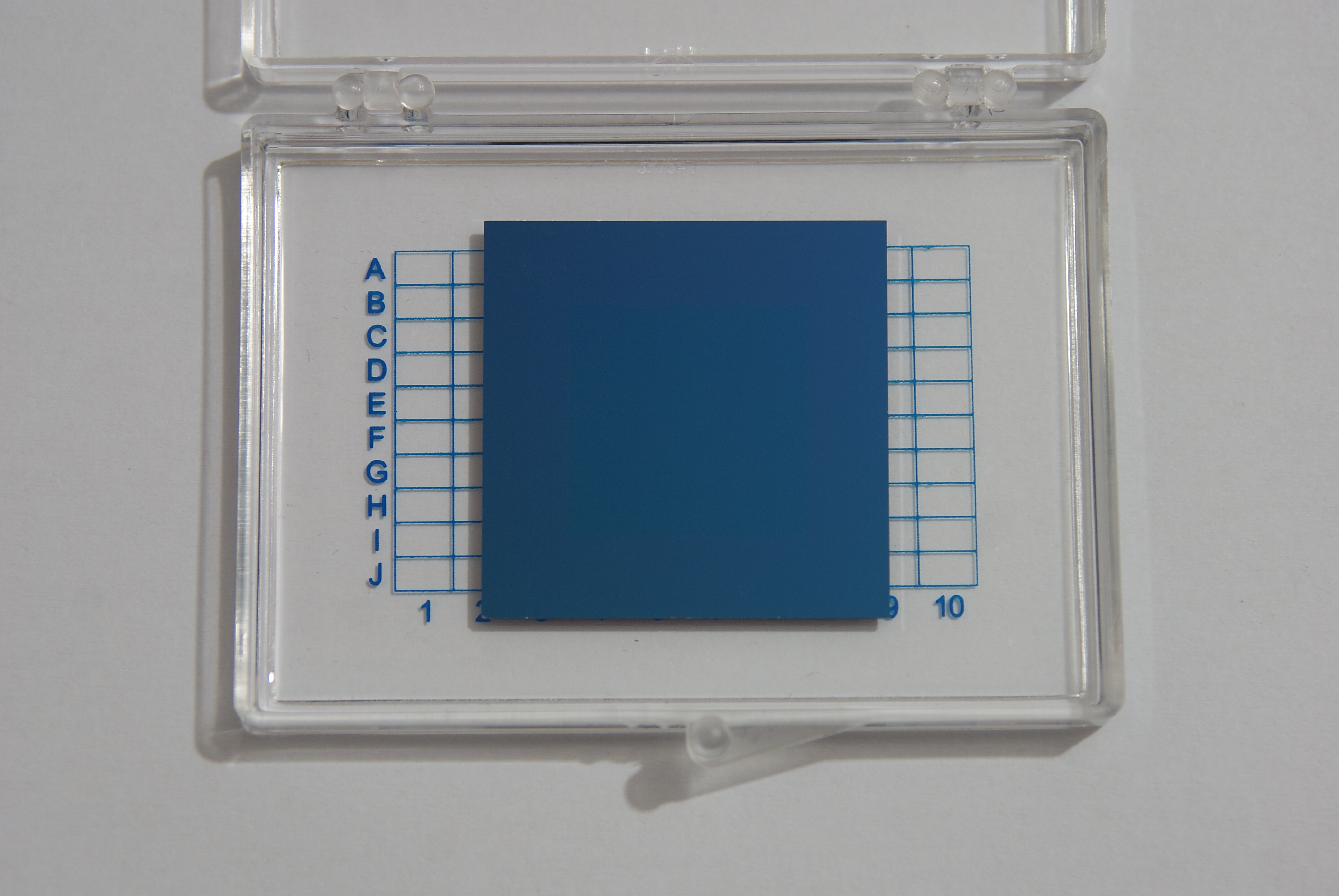
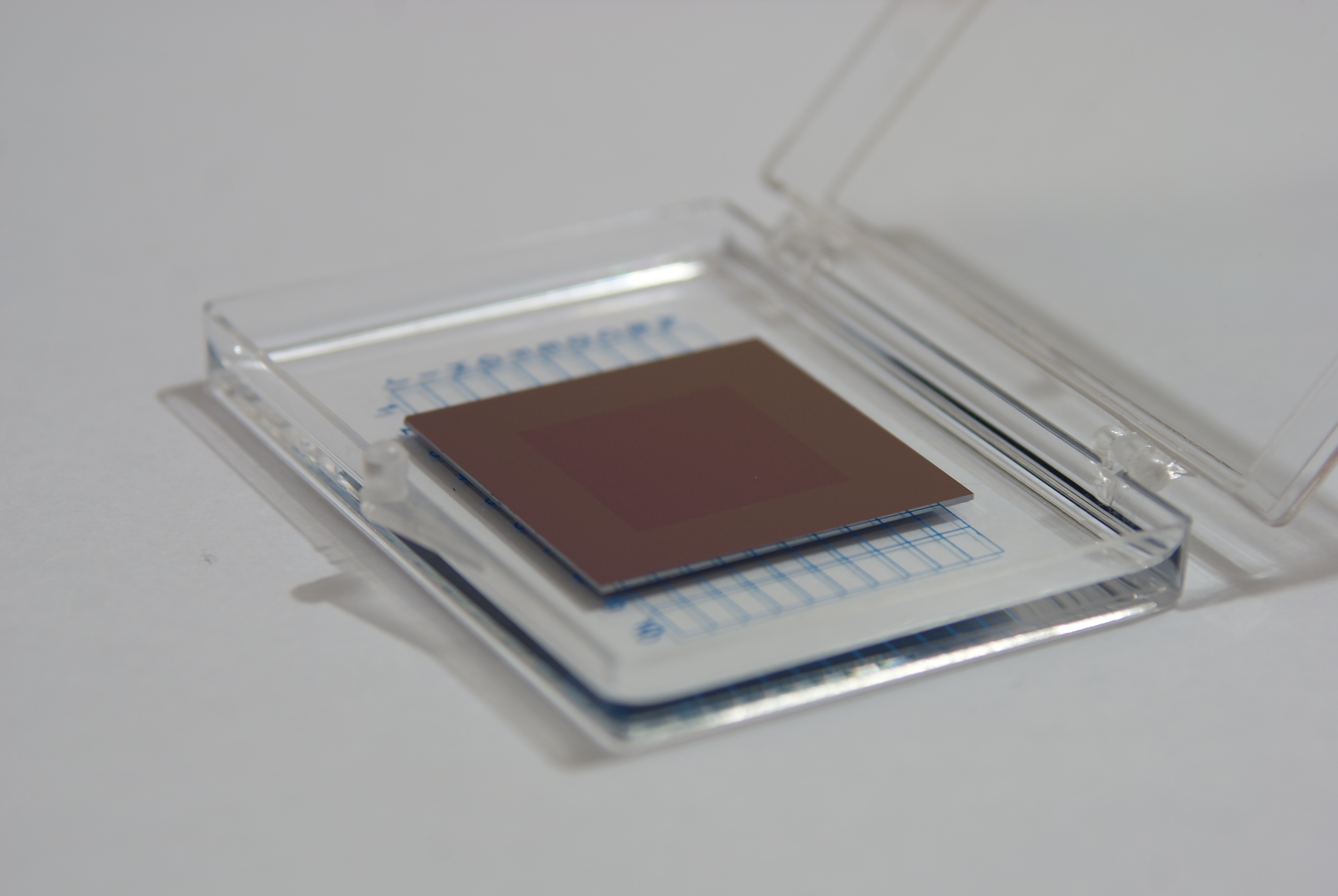
Images of CVD Graphene on SiO2 (Substrate is usually larger than the Graphene film, i.e., the SiO2/Si substrate is 1.5cm x 1.5cm for a 1cm x 1cm CVD graphene film.)
.jpg)
Raman Spectrum for Graphene-SiO2
-7cmx7cm.jpg)
CVD Graphene on SiO2 (4 inch) & The size of the graphene is 7cm x 7cm
Conditions for safe storage
Keep the products in a dry and low oxygen (or oxygen-free) container at moderate temperature (<30°C).
The products and services ACS Material is supplying include:
- Super large size graphene on copper foil up to 30cmx20cm
- Double or multi-layer graphene
- Graphene transferred onto silicon dioxide substrate
- Pretreated graphene: Graphene has been coated PMMA‚ just after some simple steps‚ you can transfer it to other different substrates
- Graphical graphene: According to graphics mask supplied by customers
- Customized service: different floors‚ different sizes of graphene; graphene transfer services; nitrogen-doped graphene; graphical graphene etc.
FAQ
Is the substrate doped? What’s the type?
It is heavily doped p-type Si wafer and the electrical resistivity is about 1-10 Ω·cm.
To check out the list of all products visit on https://yaavikmaterials.com/cvd-graphene/
To visit homepage click on https://yaavikmaterials.com/