Graphene Nanoplatelets (2-10nm)

 20000 98000 exc. gst

Graphene Nanoplatelets (2-10nm)

Types of Graphene Nanoplatelets 

Product No. Product Name Thickness Diameter Size
GNNP0051 Graphene Nanoplatelets (2-10nm thick) * 2-10nm 2~7µm 50g
GNNP0052 500g
GNNP0031 1kg
GNNP01A5 Graphene Nanoplatelets (1-2nm thick) 1-2nm 5-10µm 500mg
GNNP0201 Graphene Nanoplatelets (1-5nm thick) 1-5nm ~5µm 1g
GNNP0205 5g
GNNP0211 10g

Preparation Method

Interlayer Cleavage Method


Characterizations

Appearance

Black/Grey Powder

Diameter

2-7 μm

Thickness

2-10 nm

Specific Surface Area

20-40 m2/g

Electrical Conductivity

80000 S/m

Carbon Content

>99%

Apparent Density

0.06-0.09 g/ml

Water Content

<2 wt.%

Residual Impurities

<1 wt.%

Particle Size Distribution

D10=13.56 μm

D50=48.93 μm

D90=122.2 μm

To check out the list of all products visit on https://yaavikmaterials.com/nanoparticles-2/

To visit homepage click on https://yaavikmaterials.com/

SKU: GNNP0051 Category: Tag:

Description

Graphene Nanoplatelets (2-10nm)

Graphene Nanoplatelets (2-10nm) -The material synthesized in fully controlled environment and with proven parameters gives you the best desired results. For more information and customized requirements contact info@yaavikmaterials .com

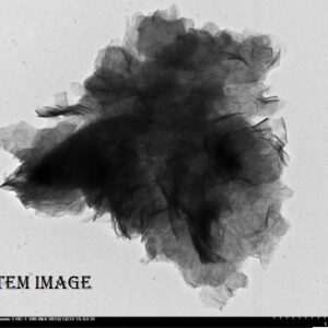
It consist of stacks of multi-layer graphene sheets in a platelet morphology‚ with a high aspect ratio (width–to-thickness).

True density: 2.3g/cm3

Bulk Characteristics

Appearance Carbon Content Bulk Density Water Content Residual Impurities
Black and Grey Powder >99% ~0.10 g/ml <2 wt% <1 wt%

Physical Properties

Diameter Thickness Specific Surface Area Electrical Conductivity Tensile Strength
2-7 μm 2-10 nm 20-40 m2/g 80000 S/m 5 Gpa
Structure Features: The layered structure is as same as graphite crystal


The product is also available on https://www.yaavikmaterials.org/  , https://yaavikmaterials.in/

Additional information

Packaging

1 Kg, 50 gm, 500 gm

Reviews

There are no reviews yet.

Be the first to review “Graphene Nanoplatelets (2-10nm)”

Your email address will not be published. Required fields are marked *