CVD Method Monolayer WSe2
₹ 185000 exc. gst
CVD Method Monolayer WSe2
YAAVIK MATERIALS AND ACS MATERIALS PRESENTS CVD Method Monolayer WSe2 in India.
Product Detail
CAS-No.: 12067-46-8 (WSe2); 60676-86-0 (SiO2)
CVD monolayer WSe2 on SiO2 substrate is just one of many advanced 2-D materials supplied by us. WSe2 is also known by several other names, including:
- Tungsten selenide
- Tungsten diselenide
- Tungsten (IV) selenide
Tungsten selenide is a member of the group-VI transition metal dichalcogenides, an important class of inorganic two-dimensional materials used in a variety of applications, including photovoltaics, lithium-ion batteries, and FETs, to name a few. WSe2’s most distinguishing feature is its low thermal conductivity; this stability makes it an efficient semiconductor and an excellent candidate for improving solar cell technology. Monolayers of WSe2 are virtually transparent. Studies have demonstrated that 95% of incident light passes through WSe2 film and the remaining is converted to electricity. Adjacent metal electrodes can change the material from p-type to n-type, allowing potential devices to have tunable band gaps and to be able to produce varying LED colors with just one material. WSe2’s low thermal conductivity results in a very efficient system.
Find high-quality monolayer CVD WSe2 with us.
1. Preparation Method
CVD Method
2. Characterizations
| Substrate: |
SiO2 |
| Size: |
9 mm*9 mm |
| Thickness: |
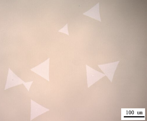
0.6-0.8 nm |
| Diameter range: |
20-50 μm |

Typical Microscope Image of Monolayer WSe2 on SiO2 (20-50μm)
3. Application Fields
An excellent device material for studying the number of layers and fluorescence effects.
To check out the list of all products visit on https://yaavikmaterials.com/graphene-like-materials/
To visit homepage click on https://yaavikmaterials.com/


Reviews
There are no reviews yet.